No products in the cart.
CVD Diamond Wafers: The Crystal Revolution in Tech
CVD diamond wafers are redefining technology with unparalleled hardness, thermal conductivity, and quantum potential. From high-performance electronics to sustainable innovation, discover how these lab-grown diamonds are revolutionizing industries.
In a world where cutting-edge technology is reshaping how we live, work, and connect, certain breakthroughs are quietly but profoundly altering the landscape. One such innovation is the Chemical Vapor Deposition (CVD) diamond wafer—a product that combines the elegance of diamonds with the transformative power of advanced science. Though lesser-known outside specialist circles, these diamond wafers are poised to influence industries ranging from semiconductors to quantum computing.
What Are CVD Diamond Wafers?
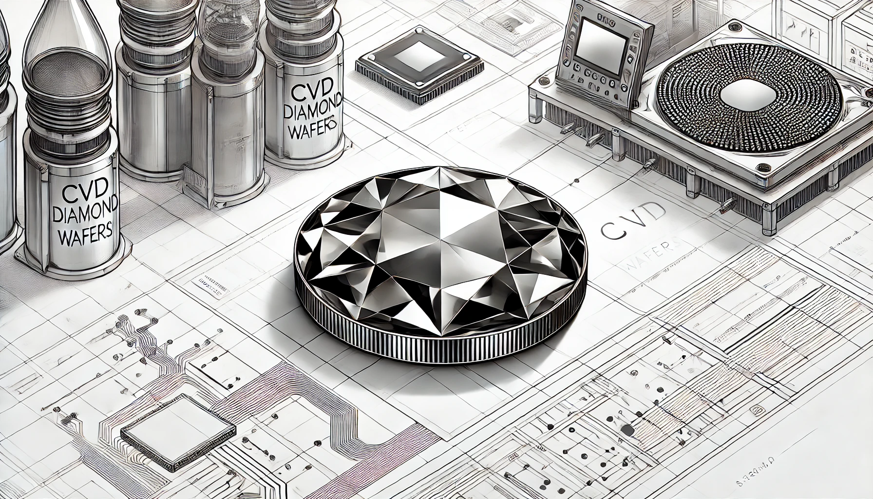
CVD diamond wafers are synthetic diamonds created in a laboratory using a method called Chemical Vapor Deposition. Unlike mined diamonds, these are grown by depositing carbon atoms layer by layer on a substrate in a controlled environment. The result? A diamond that boasts nearly identical physical and chemical properties to its natural counterpart but with the added advantage of being customizable for various applications.
Think of it as the difference between natural wood and engineered timber—both are structurally strong, but one is optimized for purpose.
Why It Matters
The significance of CVD diamond wafers lies in their exceptional properties:
 Communication
NLP: Awaken the Giant Within
Career Ahead NLP distils the idea why we are all the sum of our conditioning, as also beliefs. The idea…
Read More →Quantum Potential: Unique quantum properties, such as nitrogen-vacancy centers, position them as a frontrunner in the development of quantum computing and sensing.
- Unmatched Hardness: Diamonds are the hardest known material, and CVD wafers retain this characteristic, making them invaluable for high-stress industrial applications.
- Thermal Conductivity: With a thermal conductivity exceeding 2,000 W/mK—far superior to copper—CVD diamond wafers are critical for heat dissipation in high-performance electronics.
- Optical Clarity: Transparent from ultraviolet to infrared light, these wafers are indispensable for advanced optical systems like lasers and spectroscopy.
- Quantum Potential: Unique quantum properties, such as nitrogen-vacancy centers, position them as a frontrunner in the development of quantum computing and sensing.
Applications: Beyond the Jewelry Store
While diamond jewelry has long dominated public perception, CVD diamond wafers are making headlines in the tech world for their versatility:
- Semiconductors: As traditional silicon chips approach their physical limits, diamond wafers are emerging as an alternative for producing smaller, faster, and more efficient electronic devices.
- Quantum Computing: These wafers are being used to create qubits—the building blocks of quantum computers—offering the stability needed for this revolutionary technology.
- Optical Systems: From high-power laser lenses to infrared cameras, the optical applications of diamond wafers are vast and growing.
- Thermal Management: Their superior heat conduction makes them ideal for cooling high-power components in electric vehicles, data centers, and satellite systems.
The Billion-Dollar Industry
The CVD diamond market is growing rapidly. Valued at approximately $400 million in 2021, it is projected to reach $910 million by 2032, according to market reports. Companies like Element Six, a subsidiary of De Beers Group, and Diamond Foundry, backed by high-profile investors like Leonardo DiCaprio and Fidelity Investments, are leading the charge in this domain.
Governments are also taking notice. In 2024, the U.S. allocated a $750 million grant to support advancements in wafer technology, highlighting its strategic importance in sectors like renewable energy and defense.
Opportunities and Challenges
Opportunities
- Sustainability: Unlike traditional mining, CVD diamonds are grown in labs with significantly reduced environmental impact. This positions them as a sustainable alternative in a world increasingly conscious of its carbon footprint.
- Market Expansion: The integration of CVD diamond wafers into mainstream electronics and quantum computing could open up trillion-dollar markets.
- Versatility: Their applications span multiple industries, from medical tools to aerospace engineering, ensuring a wide revenue stream.
Challenges
- Production Complexity: Growing high-quality CVD diamonds is a time-intensive and technologically demanding process.
- Consumer Skepticism: The luxury market remains divided, with natural diamonds still perceived as more valuable.
- Regulatory Oversight: As lab-grown diamonds become more prominent, ensuring transparency in labeling and marketing will be crucial to maintaining consumer trust.
The Ethical Angle
CVD diamonds are reshaping the ethical debate surrounding diamond production. Traditional diamond mining has long been associated with environmental degradation and human rights abuses. Lab-grown diamonds, on the other hand, bypass these concerns. By eliminating the need for mining, they offer a path toward a more responsible and transparent supply chain.
 AI
AIThe Human Touch: Will AI Journalism Replace Us?
As AI technology transforms journalism, the question remains: can machines truly replace the human touch in storytelling?
Read More →Blockchain technology is further enhancing this transparency, enabling companies to provide customers with detailed provenance data for each diamond wafer or gem.
What Lies Ahead
The future of CVD diamond wafers is as dazzling as the material itself. As researchers continue to unlock new applications, these wafers could redefine what’s possible in technology. Imagine smartphones that never overheat, quantum computers solving problems in seconds, or telescopes peering deeper into the cosmos—all powered by the humble but mighty diamond wafer.
What Lies Ahead The future of CVD diamond wafers is as dazzling as the material itself.
For those entering the workforce or seeking to pivot careers, this field represents a burgeoning opportunity. Whether in engineering, materials science, or sustainability consulting, the diamond wafer industry offers a wealth of possibilities.
Closing Thought
Diamonds have always symbolized durability and brilliance, but their next chapter might be their most revolutionary yet. As the world grapples with challenges like energy efficiency, computing limits, and sustainability, CVD diamond wafers are stepping into the spotlight—not as a luxury, but as a necessity.
 Career Challenges
Economic Concerns and Public Sentiment: Insights from Indonesia
Social inequality and corruption are influencing job market perceptions in Indonesia, as revealed by Ipsos research, highlighting urgent needs for…
Read More →Tomorrow’s innovations are being built on today’s breakthroughs. In the case of CVD diamond wafers, it seems the future is indeed crystal clear.