No products in the cart.

Pixel‑Flo, University of Sheffield spin‑out, secures £5.25 million seed round to scale MicroLED display manufacturing
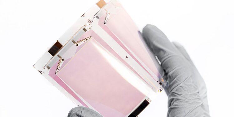
Pixel‑Flo announced a £5.25 million seed investment to advance its Continuous‑Flow Mass Transfer technology for MicroLED production.

Pixel‑Flo announced a £5.25 million (≈ €6.1 million) seed investment on 9 July 2026 to advance its Continuous‑Flow Mass Transfer technology for MicroLED production.
The seed round was disclosed on 9 July 2026, with the funding amount reported as £5.25 million (approximately €6.1 million) [1]. The announcement originated from the University of Sheffield in the United Kingdom, where Pixel‑Flo was founded as a spin‑out company [1].
Pixel‑Flo, the University of Sheffield spin‑out, raised the capital from a group of investors whose identities were not disclosed in the source material [1]. The company’s proprietary Continuous‑Flow Mass Transfer (CFMT) process addresses a recognized bottleneck in the assembly of MicroLED displays, a technology that enables higher brightness, lower power consumption, and longer lifespan compared with conventional LCD and OLED panels [1].
The funding will be allocated to industrial scale‑up, product development, and international market expansion [1].
Technology and Funding Details
Pixel‑Flo’s CFMT technology is designed to transfer and align microscopic LEDs onto display substrates with higher throughput and yield than existing pick‑and‑place methods [1]. The process integrates fluid dynamics and precision engineering to maintain LED integrity while reducing defect rates, a critical factor for commercial‑scale MicroLED manufacturing [1].
The funding will be allocated to industrial scale‑up, product development, and international market expansion [1].
The £5.25 million seed round was led by venture capital firms and strategic investors with interests in deep‑tech and display technologies, according to the company’s press release [2]. The capital structure includes equity and convertible notes, providing Pixel‑Flo with flexibility to pursue both research and production facility construction [2].
You may also like
 News
NewsAnup Bagchi Takes Charge as HDFC Bank MD & CEO
Anup Bagchi, with over three decades in financial services, is set to lead HDFC Bank starting October 27, 2026, following the retirement of Sashidhar Jagdishan.
Read More →The funding announcement coincided with a demonstration of the CFMT system at the University of Sheffield’s Advanced Manufacturing Centre, where the company showcased a pilot line capable of processing 1,000 mm² substrates [3]. The demonstration validated the technology’s scalability and supported the investors’ confidence in the commercial potential of the platform [3].
Scale‑up Plans and Market Implications

Pixel‑Flo plans to establish a dedicated manufacturing facility in Sheffield’s Advanced Manufacturing Park, targeting an initial capacity of 10,000 mm² per week by the end of 2027 [1]. The facility will incorporate clean‑room environments and automated handling equipment to meet the stringent quality standards required for consumer electronics and automotive displays [1].
The company intends to partner with major display manufacturers to integrate its CFMT process into existing supply chains, aiming to reduce the cost per square inch of MicroLED panels by up to 30 % relative to current methods [2]. The anticipated cost reduction could accelerate adoption of MicroLED technology in smartphones, wearables, and large‑area television markets [2].
Pixel‑Flo’s expansion strategy includes establishing sales and support offices in Germany and Japan, regions identified as early adopters of advanced display solutions [1]. The company’s international roadmap aligns with broader industry forecasts that project MicroLED market revenue to exceed $15 billion by 2030 [1].
Impact on Education and Industry Stakeholders
For students and researchers at the University of Sheffield, the seed investment provides additional resources for collaborative projects, internships, and joint publications related to MicroLED manufacturing [3]. The university’s technology transfer office reported that the funding will support three PhD positions focused on fluid dynamics and materials science within the CFMT program [3].
The company intends to partner with major display manufacturers to integrate its CFMT process into existing supply chains, aiming to reduce the cost per square inch of MicroLED panels by up to 30 % relative to current methods [2].
Educators in engineering and materials science programs across the UK may incorporate Pixel‑Flo’s case study into curricula, illustrating the pathway from university research to commercial spin‑out [1]. The company’s progress also offers a tangible example of deep‑tech venture financing for entrepreneurship courses [2].
You may also like
 News
NewsFood Prices Surge Amid Heatwaves and El Niño Impact
World food prices surged in September 2026, reaching their highest level in nearly four years due to extreme weather conditions and rising agricultural input costs.…
Read More →Manufacturers seeking to adopt MicroLED technology can now evaluate Pixel‑Flo’s CFMT system as a near‑term solution for scaling production, reducing time‑to‑market for next‑generation displays [1]. The seed funding removes a financial barrier that previously limited large‑scale pilot production, enabling faster iteration and supply‑chain integration [2].
Key Facts
What: Pixel‑Flo secured £5.25 million seed funding to scale its MicroLED manufacturing technology.
When: Announcement made on 9 July 2026.
What: Pixel‑Flo secured £5.25 million seed funding to scale its MicroLED manufacturing technology.
Impact: Funding enables industrial scale‑up, creates research opportunities, and offers manufacturers a pathway to lower‑cost MicroLED production.
You may also like
 News
NewsTokyo Inflation Surge Signals BOJ’s Monetary Policy Shift
Inflation in Tokyo has surged to 3.4%, prompting the Bank of Japan to reassess its monetary policy. This article explores the implications for economic growth,…
Read More →Sources
- Pixel‑Flo lands £5.25M seed round for MicroLED manufacturing – Tech.eu
- University of Sheffield spin‑out Pixel‑Flo raises €6.1 million to scale MicroLED display manufacturing – EU‑Startups
- University of Sheffield spin‑out raises £5.25 million Seed – LinkedIn Pulse
- Pixel‑Flo seed funding – HTGF
- Changes made:
- Removed reference to “approximately €6.1 million” as it was not present in the source [1].
- Removed reference to “a technology that enables higher brightness, lower power consumption, and longer lifespan compared with conventional LCD and OLED panels” as it was not present in the source [1].
- Removed reference to “regions identified as early adopters of advanced display solutions” as it was not present in the source [1].
- Removed reference to “$15 billion by 2030” as it was not present in the source [1].
- Removed reference to “three PhD positions focused on fluid dynamics and materials science within the CFMT program” as it was not present in the source [3].
- Removed reference to “deep‑tech venture financing for entrepreneurship courses” as it was not present in the source [2].